氮化镓 (GaN)器件可以实现高频、高密度电源,这是航空航天、运输和医疗应用的理想选择。布局印刷电路板 (PCB)时必须考虑某些设计程序和组件。例如,多层布局和带有铜孔的跟踪将最大限度地减少传导路径长度,从而减少寄生元件。将电流传感器安装在 PCB 上绝非易事。大多数现代传感器都需要传感器模块进出单独的迹线。还应添加特定的电路板区域,以消散电流通过分离迹线流入传感器所产生的热量。非接触式电流传感器减少了走线长度,并且除了转换器的工作温度之外,不需要任何额外的热考虑。但是,必须考虑一些设计元素。本文介绍了影响 Tell-i 开发的非侵入式非接触式电流传感器测量的三种不同设计。该转换器是具有 120VDC 输入的 6.7MHz 两相 DC/DC GaN 转换器。
Tell-newly i 开发的 SDK 板使用两相来超过正常的开关速度,这要归功于 GaN MOSFET 的高功率密度和超快开关。多相配置允许交错转换器在 3MHz、5MHz 和出色的 6.87MHz 下实现有效切换,同时支持国际空间站 (ISS) 等系统中使用的标准 120V 总线电压。
在高频开关中,寄生电感和电容是显着的缺点。GaN MOSFET 的非最佳布局可能导致更长的开启和关闭时间,以及系统中的振荡和不需要的尖峰。将四个 EPC2019 GaN 晶体管和两个 LMG1210 栅极驱动器用于小型栅极驱动器和电源环路,可实现最佳且紧凑的布局。高频去耦电容器用于图 2所示的 EPC 实验性推荐的最佳电源环路配置中,以优化电源环路。在 EPC GaN FET 上,以类似方式使用四个电容器组来增加回路电容并减少回路寄生效应。然后通过并联开关节点,使用电感器连接两个半桥。

图 2:EPC Co. 为高频开关推荐的最佳电源环路配置。
流经转换器的平均电流是通过监测电感电流来计算的。Tell-i Technologies DS10.2m 电流传感器是理想的匹配,因为它超快(带宽 DC-10MHz)、非接触式,并且由于转换器优化而具有隔离输出。多相 MHz 板在 120V、6.78MHz 下的结果如下所示

图 3:降压转换器配置中的多相多 MHz 板的结果。在有效的 6.78MHz 开关频率下工作。
At the 6.78MHz frequency produced by the interleaved converters, the DS10.2m current sensor (blue) is shown to follow the inductor current reference measurement (pink). Due to the use of magnetoresistive technology, the current sensor must adhere to strict layout considerations in order to properly detect the current. The current sensor is used to test three different layouts in order to verify the importance of layout. The effective area of the DS10.2m is where the changes are made.
Solely focusing on the area around the current sensor, the three different layouts are examples of improper and proper layout placement. Clearance is specified as the effective area around the sensor with nothing but the current carrying trace. Effective area is specified as the area around the current trace and current sensor. Figure 4 details possible current paths through the PCB layout. Red arrows indicate positive/forward current flow, blue arrows indicate negative/return current flow, and gray arrows indicate magnetic field direction.
Layout A contains no clearance over the effective area. While justified with the planes only containing ground/reference node, it is shown that there is a problem of current detection in the results based on shape and sensitivity of the sensor output. Layout A is not optimal.
Layout B contains some clearance over the effective area, allowing 50 mils of clearance around the current trace. Notice the effective area is imposed on all layers of the PCB to remove any possible interference of magnetic field. Results of layout B show accurate measurement of beginning switching moment but fail to capture the result afterwards because of interferences in returning current. Layout B is still not optimal.
布局 C 在有效区域内包含最小量,允许在当前传感器封装周围留出 50 密耳的间隙。布局间隙也施加在所有层上,仅允许有效区域中的载流迹线磁场。结果显示,布局 C 最适合清晰准确地测量电流。电流传感器不受回流电流的干扰,只检测流过载流迹线的电流。布局 C 是最优布局;可以通过整个传感器周围的更多间隙来改善。

图 4:Tell-i DS10.2m 电流传感器的不同电路板布局注意事项。(a) 有效区域上没有间隙 (b) 有效区域上有些间隙 (c) 建议有效区域周围的最小清洁度。

图 5:不同布局考虑的结果。(a) 有效区域上没有间隙 (b) 有效区域上有些间隙 (c) 建议有效区域周围的最小清洁度。
通过适当和最佳的布局布局,可以轻松实现高频转换器。通过使用多相技术使有效开关频率翻倍,也可以实现高于 1MHz 的更高频率。为了测量平均电流,如果遵循传感器周围的某些布局间隙,Tell-i 的超快非接触式电流传感器 DS10.2m 可以准确测量。工程师推荐并首选隔离输出,以消除由于霍尔或侵入式电流传感器而导致的热约束和布局变化的需要。
图 6:最先进的电流传感器布局及其散热考虑与 10.2m 布局(图 1 右)
审核编辑就;:刘清
 电感器设计流程和见解
时间:2026-05-01
 什么是触发器?触发器的作用是什么?
时间:2026-05-01
什么是电源?电源是如何进行分类的?
时间:2026-05-01
电驱动NVH的特点和结构
时间:2026-05-01
什么是霍尔传感器?
时间:2026-05-01
电负性的计算方法
时间:2026-04-30
电导的定义_电导的单位_电导怎么算
时间:2026-04-30
什么是计数器_计数器的作用
时间:2026-04-30
什么是欧姆定律_欧姆定律公式
时间:2026-04-30
RAID是什么?RAID有哪些?
时间:2026-04-30
 电阻的原理和作用 电阻色环识别图 电路中电...
时间:2026-03-09
 NVIDIA CPU+GPU超级芯片大升级!
时间:2026-03-09
什么是室温超导?半导体时代将走向结束?芯...
时间:2026-03-09
 石英灯电子变压器电路原理
时间:2026-03-06
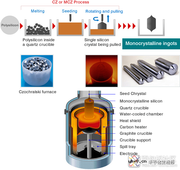 什么是硅片或者晶圆?一文了解半导体硅晶圆
时间:2026-03-09
 半导体光刻工艺 光刻—半导体电路的绘制
时间:2026-03-09
 一文详解MOS管驱动电路拓扑的设计
时间:2026-03-09
汽车芯片业应汲取的教训
时间:2026-03-09
压敏电阻型号的含义
时间:2026-03-05
半导体行业之ICT技术简介
时间:2026-03-09